Fabrication of semiconductor nanoparticles having variable optical gaps
- Development of semiconductor nanomaterial applicable to photocatalyst
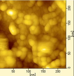
Our group found that nanoparticles of 10 nm in diameter were formed when
high-density plasma regions were generated in pores of
the porous aluminum plate set between a cathode and an anode (inside
of plasma) during plasma synthesis of a-C having variable band gaps.
a-C semiconductor nanoparticles of which wavelength are selective
are expected to have widespread applications for future energy industry
or electro devices, such as photocatalytic fine particles and quantum
dot solar cells.
References
1) Kensuke HONDA and Ryutaro KOBAYASHI, Electrochemistry, 88(5), 397–406
(2020)
“Fabrication of C-rich a-SiC Semiconductor Nanoparticles Having
Variable Optical Gaps and Particle Sizes Using High-density Plasma
in Localized Area”
Patent
1) JP, 6815016, B
[Japanese Patent Application No.] 2015-045860
[Inventor] Kensuke Honda
[Title of the invention] PRODUCTION METHOD OF AMORPHOUS CARBON NANOPARTICLE
AND AMORPHOUS CARBON NANOPARTICLE
[Applicant] Yamaguchi University
[Date of filing] 6, March, 2015