Fabrication of amorphous carbon-based semiconductor capable of controlling
its optical gap by incorporating
two different foreign atoms − Development of semiconductor material for solar cells to achieve high
conversion efficiency
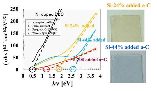
This is amorphous carbon (a-C) based semiconductor material of which optical
gaps are controllable as desired, from 1.25 to 2.76 eV.
Silicone and nitrogen atoms are simultaneously incorporated in the
a-C using plasma CVD method.
Si/C ratio can be changed by varying composition of source materials.
Consequently, optical gaps of the a-C can be controlled to the desired
value. When Si ratio of Si-added N-doped a-C film is set at Si:C:N = 18:68:1,
the color of the film becomes yellow and functions as n-type semiconductor
(an optical gap of 1.78 eV).
When Si atom% is set at 41, it becomes blue and functions as n-type
semiconductor (an optical gap of 2.76 eV).
References
1) Kensuke Honda, Kohsuke Yoshinaga and Yoshiya Nagata, ECS J. Solid State
Sci. Technol., 5, pp. 590-597 (2016).
“ Amorphous Carbon-Based Semiconductor Capable of Controlling Its
Optical Gap and Conductivity by Incorporating Silicon and Nitrogen Atoms”
Patent
1) JP, 6167263, B
[Japanese Patent Application No.] 2013-043709
[Inventor] Kensuke Honda
[Title of the invention] An n-TYPE SEMICONDUCTOR COMPOSED OF NITROGEN-CONTAINING AMORPHOUS SILICON
CARBIDE
AND ITS MANUFACTURING METHOD
[Applicant] Yamaguchi University, SAMCO INC.
[Date of filing] 6, March, 2013
2) WO-A1-2013/065315
[Application No.] JP2012007029
[Japanese Patent No.] JP, 6083676, B
[Japanese Patent Application No.] 2013-541636
[Inventor] Kensuke Honda
[Title of the invention] THE METHOD OF FABRICATING N-TYPE SEMICONDUCTOR
AND N-TYPE SEMICONDUCTOR ELEMENTS
MADE OF AMORPHOUS SILICON CARBIDE DOPED WITH NITROGEN.
[Applicant] Yamaguchi University
[Date of filing] 1, November, 2012